


Researchers from Saudi Arabia’s King Abdullah University of Science and Technology (KAUST) have teamed up with two premier European technology universities in a study that could significantly impact the future of renewable energy.
KAUST teamed up with Delft University of Technology (TU Delft) and Ludwig-Maximilians-Universität München (LMU Munich) and demonstrated that controlling nanoscale surface roughness at the recombination layer in perovskite-silicon tandem solar cells can improve performance by as much as 33.2 per cent.
This is way more than the certified efficiency of 29.5 per cent for a perovskite-silicon tandem cell achieved by researchers at Oxford PV in 2024.
Next-generation solar cell design
Unlike a traditional solar cell, or a photovoltaic cell, which was primarily made of a single mineral – crystalline silicon or cadmium telluride thin-film – the perovskite-silicon tandem solar cell are different in both their structure and manufacturing process.
Perovskite refers to a class of materials that share the same crystal structure as the mineral calcium titanium oxide (CaTiO3) and are extremely promising for solar cell applications due to their exceptional light absorption, high charge-carrier mobility, and ease of fabrication.
Unlike silicon cells, which require high-temperature processing and energy-intensive purification, perovskite films can be deposited using low-cost solution-based methods, such as spin-coating or inkjet printing, at relatively low temperatures. This unique characteristic makes perovskite solar cells potentially cheaper and more versatile for a range of applications.
Traditional silicon solar panels have achieved efficiencies of around 20–23 per cent in commercial products, but perovskite solar cells promise a lot more and have achieved upto 30 per cent efficiency in laboratory conditions.
The research team has shown that perovskite-silicon tandem solar cells have surpassed the efficiency of single-junction devices. While most research efforts have optimised the perovskite top cell and its interfaces, the silicon bottom cell has remained relatively underexplored even though it plays a crucial role on the overall device performance.
Surface texture key to efficiency
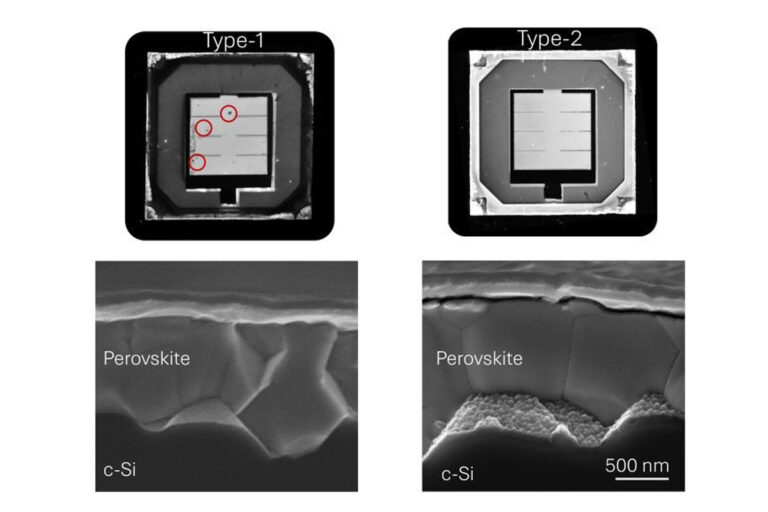
The study of the three leading universities has found that nanoscale surface roughness originating from the top layers of the bottom cell and transferred to the recombination junction significantly influences key processes such as self-assembled monolayer anchoring, perovskite crystallisation, and interface quality.
Nanoroughness in photovoltaic (PV) cells refers to engineered, small-scale surface textures or irregularities with dimensions typically less than 100 nanometers.
The deposition of and plasma treatments on hydrogenated nanocrystalline silicon layers, by altering the nanoscale surface roughness of textured silicon surfaces, yielded improved fill factors and higher device efficiencies of up to 32.6 per cent.
According to the International Energy Agency (IEA), the cost of solar photovoltaic electricity has fallen by 82 per cent over the past decade, driven largely by improvements in manufacturing and scale. The introduction of perovskite technology could accelerate this trend, making solar installations even more affordable.
Erkan Aydin, co-corresponding author of the research, told pv magazine: “The key novelty of our study lies in demonstrating that the nanoroughness of the recombination junction can be deliberately engineered to significantly improve the performance of perovskite-silicon tandem solar cells.
“By systematically tuning the surface morphology at the nanoscale, we improved electrical contact quality and reduced recombination losses, which led to reproducible and higher efficiency results.
Compatible with silicon heterojunctions
This provides a new design parameter that is compatible with existing silicon heterojunction technology.
“Our design strategy complements these efforts by addressing the physical structure of the recombination junction itself. Importantly, this approach does not require new materials or complex processing steps, making it highly synergistic with established silicon heterojunction and perovskite fabrication routes.”
Looking ahead, the KAUST Photovoltaics lab (KPV-lab) is focused on bringing emerging photovoltaic technologies closer to the market.
Stefaan De Wolf, co-corresponding author, told the pv magazine: “We work on perovskite and silicon technologies in single-, dual- and triple-junction configurations for various applications. Tailoring PV cell and module technologies for deployment in hot and sunny climates holds particular interest.”
Follow us on